Heterostructure growth
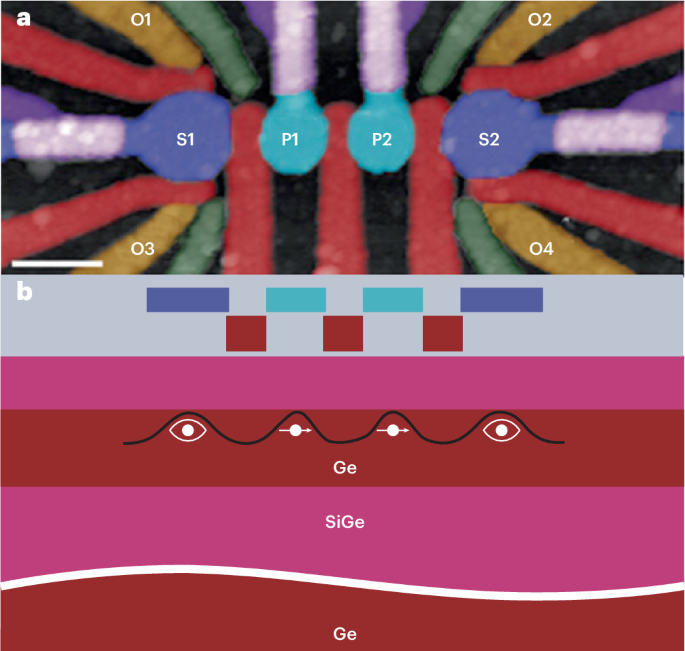
The Ge/SiGe heterostructure material is grown using reduced-pressure chemical vapour deposition in an ASMI Epsilon 2000 reactor. Starting from a Ge wafer, a 2.5 μm strain-relaxed Si(1–x)Gex buffer is grown at a temperature of 800 °C with a final Ge concentration of x = 0.83 using three grading steps (1 − x = 0.07, 0.13, 0.17). We lower the growth temperature to 500 °C for the growth of the final 200 nm of the SiGe buffer layer, the 16 nm Ge quantum well, the 55 nm SiGe barrier layer and the sacrificial passivated Si cap layer. As measured in ref. 21, this heterostructure supports a 2D hole gas with a high maximum mobility of 3.4(1) × 106 cm2 V–1 s–1 and a low percolation density of 1.22(3) × 1010 cm−2. The threading dislocation density is 6(1) × 105 cm−2, nearly an order of magnitude lower than for the growth of Ge quantum wells with similar strain starting from a Si wafer.
Device fabrication
All devices are fabricated on the same Ge/SiGe heterostructure on a Ge wafer as that measured in ref. 21. The two linear array quantum dot devices are fabricated with multiple layers of Ti/Pd and platinum–germanosilicide (PtSiGe) ohmic contacts. These are defined by electron-beam lithography and created by thermally diffusing Pt at a temperature of 400 °C. A first layer of Ti/Pd (3/17 nm) barrier gates is separated from the heterostructure by a 7 nm Al2O3 insulating oxide grown using atomic layer deposition. A second layer of Ti/Pd (3/37 nm) plunger gates is created and separated by 5 nm of Al2O3 from the first layer of barrier gates. Details for the fabrication of the 3–4–3 device (2D quantum dot array) can be found in ref. 6.
Flank method electrical characterization of quantum dots
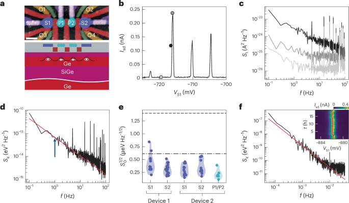
We cool multi-hole quantum dots defined underneath the charge sensor or plunger gates of a device in a Leiden cryogenic dilution refrigerator operating at a mixing chamber base temperature of 70 mK. To measure the charge noise using the flank method, we first set a source–drain bias (Vsd) of 0.1 mV across the device and subsequently tune the surrounding gates until we measure a current of 1 nA through the device. We define a multi-hole quantum dot underneath a sensor or plunger gate by fine tuning the barrier gates surrounding the gate of interest until we observe a spectrum of Coulomb peaks. We then measure the source–drain current Isd on the left flank of the Coulomb peak where the slope ∣dIsd/dVsd∣ of the Coulomb peak is the largest at a rate of 2 kHz for a duration of 100 s using a Keithley DMM6500 multimeter. To calculate the current power spectral density SI, we first split each 100 s current trace into ten segments of 10 s each, and subsequently average over the current power spectral densities (\({S}_{{{I}}}=1/N\mathop{\sum }\nolimits_{i = 1}^{N}{S}_{{{I}}}^{i}\)) that we evaluate from each segment. For each Coulomb peak that we analyse, we convert the current power spectral density SI into charge noise power spectral density Sϵ using15
$${S}_{\epsilon }=\frac{{a}^{2}{S}_{{{I}}}}{| {\rm{d}}{I}_{{\rm{sd}}}/{\rm{d}}{V}_{{\rm{S}}}{| }^{2}}\,,$$
(1)
where VS is the sensor voltage and a is the lever arm extracted from the analysis of the corresponding Coulomb diamond.
Coulomb peak tracking
On sensor 1 of device 2, we perform an ~18 h CPT experiment tracking the current Isd through a quantum dot while continuously sweeping across the quantum dot using its plunger gate. For the four charge sensors of the 3–4–3 device, we track the reflected signal of each charge sensor for ~2 h when sweeping the sensor plunger gate voltage. We extract the position of the Coulomb peak by fitting each Coulomb peak to a hyperbolic secant function
$$y=\frac{a}{{\cosh }^{2}\left(b\,(x-{x}_{{\rm{0}}})\right)}+c\,,$$
(2)
where y reflects the measured signal, x is the sensor’s plunger gate voltage, x0 is the position for which the Coulomb peak is maximum and a, b and c are free fitting parameters. To calculate the voltage power spectral density SV from the Coulomb peak fluctuations, we split them into ten equal segments and for each segment we calculate the voltage power spectral density from a Fourier transformation. We find the charge noise power spectral density Sϵ (Fig. 3c) using the evaluated lever arm of each sensor and using
$${S}_{\epsilon }={a}^{2}{S}_{{{V}}}.$$
(3)
Voltage noise estimation on single-hole quantum dots
To estimate the voltage noise of the quantum dots where we know the exact hole occupancy, we repeatedly load a hole into a dot by continuously sweeping the plunger gate voltage under which the quantum dot is defined. We keep track of the voltage for which a hole loads into a dot by fitting each voltage sweep to a sigmoid function given by
$$y=\frac{a}{1+\exp \left(\frac{x-{x}_{{\rm{0}}}}{\tau }\right)}+b\,,$$
(4)
where y reflects the measured signal, x0 is the voltage for which a hole loads into a dot and a, b and τ are free fitting parameters. We split the voltage fluctuations into ten equal segments and calculate the voltage power spectral density SV from a Fourier transformation. The final voltage power spectral density is calculated from the average of the ten segments. Because of the complexity in determining with accuracy the lever arm of the plunger gates to the quantum dots in this regime, we maintain the metric of the charge noise in voltage, rather than in energy.
Estimation of the relative out-of-plane angle between magnetic field and substrate
We consider the average effective g-factor geff = 0.58 of the ten qubits49 and assume in-plane principal g-tensor components of gx = −gy = 0.04 (ref. 6) and an out-of-plane component of gz = 11 (ref. 26). Assuming the g-tensor axes follow the crystal directions, the effective g-factor can be written in terms of the out-of-plane angle θ and the principal components:
$${g}_{{\rm{eff}}}=\sqrt{{g}_{x}^{2}\cos {\theta }^{2}+{g}_{z}^{2}\sin {\theta }^{2}}.$$
(5)
By inverting the equation, we estimate the most plausible misalignment angle of θ = 3°.
Extraction of Rabi and Larmor frequency
We extract the Larmor frequency fL and Rabi frequency fR by fitting the data with the following functions. For the Rabi frequency we use
$$P_{\uparrow}=A\sin (2\uppi {f}_{{\rm{R}}}t+\phi )\exp (-{t}^{2}/{\tau }^{2})+C\,,$$
(6)
where P↑ represents the measured up probability and t is the duration of the microwave burst. The Rabi frequency fR, decay time τ, phase ϕ, amplitude A and offset C are free fitting parameters. The extraction of the Larmor frequency is done using
$$P_{\uparrow}=A\frac{{f}_{{\rm{R}}}^{\,2}}{{f}_{{\rm{R}}}^{\,2}+{\it{\varDelta} }^{2}}{\sin }^{2}\left(0.5t\sqrt{{f}_{{\rm{R}}}^{\,2}+{{\it{\Delta}} }^{2}}\right)+C\,.$$
(7)
Here Δ = f − fL with f the probed frequency range during measurement; t, A, fR, C and fL are free fitting parameters.
Qubit noise model
Low-frequency and hyperfine noise affecting the qubits hosted in the natural Ge/SiGe heterostructure is modelled by26
$${S}_{{f}_{{\rm{L}}}}=\frac{{S}_{{\rm{0}}}}{f}+{S}_{0,{\rm{hf}}}\exp \left(\frac{-{(\,f-{f}_{{\rm{Ge}}-73})}^{2}}{2{\sigma }_{{\rm{Ge}}-73}^{2}}\right)\,.$$
(8)
Here, S0 represents the low-frequency noise component at 1 Hz and S0,hf represents the effective strength of the hyperfine noise acting on the qubit; fGe−73 = γGe−73B is the precession frequency of 73Ge determined by its gyromagnetic ratio γGe−73 = 1.48 MHz T–1 and the magnetic field B; and σGe−73 represents the spread of the 73Ge precession frequencies. We follow the same fitting procedure as outlined in the methods of ref. 26 to extract S0, S0,hf and σGe−73.
For the fitting of the data containing influence of the 29Si nuclear spin, we expand equation (8) with a second Gaussian peak:
$$\begin{array}{ll}{S}_{{f}_{{\rm{L}}}}=\frac{{S}_{{\rm{0}}}}{f}&+{S}_{0,{\rm{hf}}}^{{\rm{Ge}}-73}\exp \left(\frac{-{(\,f-{f}_{{\rm{Ge}}-73})}^{2}}{2{\sigma }_{{\rm{Ge}}-73}^{2}}\right)\\ &+{S}_{0,{\rm{hf}}}^{{\rm{Si}}-29}\exp \left(\frac{-{(\,f-{f}_{{\rm{Si}}-29})}^{2}}{2{\sigma }_{{\rm{Si}}-29}^{2}}\right)\,.\end{array}$$
(9)
The fitting procedure is split into a two-stage process, where we first use equation (8) to find \({S}_{0,{\rm{hf}}}^{{\rm{Ge}}-73}\) and σGe−73. We fix these parameters and then use equation (9) to find S0, \({S}_{0,{\rm{hf}}}^{{\rm{Si}}-29}\) and σSi−29. The precession frequencies of fGe−73 and fSi−29 are also fixed.
Estimation of the hyperfine noise contribution
Using the average extracted parameters of \({S}_{0,{\rm{hf}}}^{{\rm{Ge}}-73}=1.1(3)\times 1{0}^{6}\,{{{\rm{Hz}}}^{2}} \, {{\rm{Hz}}^{-1}}\) and σGe−73 = 12(1) kHz that describe the modelled Gaussian peak in the power spectral density at the frequency fGe−73, we estimate an integrated noise of the Larmor frequency fluctuations of
$${\sigma }_{f}=\sqrt{\sqrt{2\uppi } \times {S}_{0,{\rm{hf}}}^{{\rm{Ge}}-73}{\sigma }_{{\rm{Ge}}-73}}=180(8)\,{\rm{kHz}}.$$
(10)
This sets an approximate boundary for the hyperfine-limited dephasing time of \({T}_{2}^{\,* }={(\uppi \sqrt{2}{\sigma }_{f})}^{-1}=1.25(5)\,\upmu {\rm{s}}\), qualitatively similar to what is measured experimentally, on the order of 1 μs to 2 μs (ref. 49).
We use the same procedure to assess the influence of the interaction with the 29Si nuclei in the barrier to the Ge hole spin qubits. We consider the average parameters extracted from the fits in Fig. 4, \({S}_{0,{\rm{hf}}}^{{\rm{Si}}-29}=9.0(8)\times 1{0}^{3}\,{{{\rm{Hz}}}^{2}} \, {{\rm{Hz}}^{-1}}\) and σSi−29 = 99(20) kHz, that lead to an integrated noise of σf = 47(5) kHz and a 29Si-limited \({T}_{2}^{\,* }=4.8(4)\,\upmu {\rm{s}}\).
Effective voltage noise and charge-noise-limited \({{\boldsymbol{T}}_{\mathbf{2}}}^{\mathbf{*}}\)
We assume a spatially homogeneous distribution of uncorrelated fluctuators, and exploit knowledge of the g-factor susceptibility to voltage variations in all the surrounding gates49. Considering traps under the gates the most dominant, uncorrelated noise sources, we can estimate the resulting overall g-factor susceptibility of the hole spin qubits as \(\frac{\Delta g}{\Delta V}=\sqrt{{\sum }_{i}{(\frac{\updelta g}{\updelta {V}_{i}})}^{2}}\approx 6.7\times \,1{0}^{-4}\,{{\rm{mV}}}^{-1}\), with δg/δVi the susceptibility of the g-factor g to a voltage variation on each gate i (Vi) of the twelve barrier and ten plunger gates controlling the array. The associated Larmor qubit fluctuations result then into \(\frac{\Delta {f}_{{\rm{L}}}}{\Delta V}=\frac{1}{h}\,\frac{\Delta g}{\Delta V}\,{\mu }_{{\mathrm{B}}}B\), where h is the Planck constant and μB is the Bohr magneton. For B = 117.5 mT the value of the fluctuations is ~1.1 MHz mV−1. We can then derive an effective voltage power spectral density value at 1 Hz of
$${S}_{{{V}}}=\frac{{S}_{{\rm{0}}}}{{\left(\frac{\Delta {f}_{{\rm{L}}}}{\Delta V}\right)}^{2}}=140(30)\,\upmu {{{\rm{V}}}^{2}} \, {{\rm{Hz}}^{-1}}$$
(11)
that results in an effective voltage noise of \({S}_{{{V}}}^{1/2}=12(1)\,\upmu {\rm{V}} \, {\rm{Hz}}^{-1/2}\).
We evaluate the charge-noise-limited \({T}_{2}^{\,* }\) using the extracted voltage noise amplitude of \({S}_{{{V}}}^{1/2}=12(1)\,\upmu {\rm{V}} \, {\rm{Hz}}^{-1/2}\) at 1 Hz and the effective g-factor susceptibility of \(\frac{\Delta g}{\Delta V}=6.7\times 1{0}^{-4}\,{{\rm{mV}}}^{-1}\). The dephasing time \({T}_{2}^{\,* }\) can be approximated in a quasi-static configuration by6,15,50
$${T}_{2}^{\,* }=\frac{1}{\sqrt{2}\uppi \Delta f},$$
(12)
with Δf the amplitude of the qubit frequency fluctuations due to a voltage noise with root mean square amplitude of ΔVr.m.s.
$$\Delta f=\frac{\Delta g}{\Delta V}\Delta {V}_{{\rm{r.m.s.}}}.$$
(13)
We compute ΔVr.m.s. over a period of time T assuming a power spectral density of SV/f, and integrating the noise from low-frequency and high-frequency cut-off values, fL = T−1 and fH, respectively:
$$\Delta {V}_{{\rm{r.m.s.}}}=\sqrt{\mathop{\int}\nolimits_{{f}_{{\mathrm{L}}}}^{{f}_{{\mathrm{H}}}}\frac{{S}_{{{V}}}}{f}\,{\mathrm{d}}f}=\sqrt{{S}_{{{V}}}\ln \frac{{f}_{{\mathrm{H}}}}{{f}_{{\mathrm{L}}}}}.$$
(14)
By considering realistic values of fL = 1 mHz and fH = 1 MHz, we determine \(\Delta {V}_{\rm{r.m.s.}}=54(5)\,\upmu {\rm{V}} \, {\rm{Hz}}^{-1/2}\). We then distinguish two cases. For B = 117.5 mT, the resulting fluctuations lead to Δf = 60(5) kHz and a charge-noise-limited dephasing time of \({T}_{2}^{\,* }=3.7(3)\,\upmu {\rm{s}}\). For a low magnetic field of 10 mT, we obtain an increased value of \({T}_{2}^{\,* }=44(4)\,\upmu {\rm{s}}\) due to the more than tenfold reduction in Δf.