Wu, G. et al. Ferroelectric-defined reconfigurable homojunctions for in-memory sensing and computing. Nat. Mater. 22, 1499–1506 (2023).
Google Scholar
Liu, Y. et al. Promises and prospects of two-dimensional transistors. Nature 591, 43–53 (2021).
Google Scholar
Qiu, H. et al. Two-dimensional materials for future information technology: status and prospects. Sci. China Inf. Sci. 67, 160400 (2024).
Google Scholar
Wang, C., You, L., Cobden, D. & Wang, J. Towards two-dimensional van der Waals ferroelectrics. Nat. Mater. 22, 542–552 (2023).
Google Scholar
Wang, X. et al. Interfacial ferroelectricity in rhombohedral-stacked bilayer transition metal dichalcogenides. Nat. Nanotechnol. 17, 367–371 (2022).
Google Scholar
Weston, A. et al. Interfacial ferroelectricity in marginally twisted 2D semiconductors. Nat. Nanotechnol. 17, 390–395 (2022).
Google Scholar
Deb, S. et al. Cumulative polarization in conductive interfacial ferroelectrics. Nature 612, 465–469 (2022).
Google Scholar
Van Winkle, M. et al. Engineering interfacial polarization switching in van der Waals multilayers. Nat. Nanotechnol. 19, 751–757 (2024).
Google Scholar
Wang, L. et al. Correlated electronic phases in twisted bilayer transition metal dichalcogenides. Nat. Mater. 19, 861–866 (2020).
Google Scholar
Wu, F., Lovorn, T., Tutuc, E., Martin, I. & MacDonald, A. H. Topological insulators in twisted transition metal dichalcogenide homobilayers. Phys. Rev. Lett. 122, 086402 (2019).
Google Scholar
Suzuki, R. et al. Valley-dependent spin polarization in bulk MoS2 with broken inversion symmetry. Nat. Nanotechnol. 9, 611–617 (2014).
Google Scholar
Scuri, G. et al. Electrically tunable valley dynamics in twisted WSe2/WSe2 bilayers. Phys. Rev. Lett. 124, 217403 (2020).
Google Scholar
Li, X. et al. Rhombohedral-stacked bilayer transition metal dichalcogenides for high-performance atomically thin CMOS devices. Sci. Adv. 9, eade5706 (2023).
Google Scholar
Rogée, L. et al. Ferroelectricity in untwisted heterobilayers of transition metal dichalcogenides. Science 376, 973–978 (2022).
Google Scholar
Shi, J. et al. 3R MoS2 with broken inversion symmetry: a promising ultrathin nonlinear optical device. Adv. Mater. 29, 1701486 (2017).
Google Scholar
Dong, Y. et al. Giant bulk piezophotovoltaic effect in 3R-MoS2. Nat. Nanotechnol. 18, 36–41 (2023).
Google Scholar
Yang, D. et al. Non-volatile electrical polarization switching via domain wall release in 3R-MoS2 bilayer. Nat. Commun. 15, 1389 (2024).
Google Scholar
Suh, J. et al. Reconfiguring crystal and electronic structures of MoS2 by substitutional doping. Nat. Commun. 9, 199 (2019).
Google Scholar
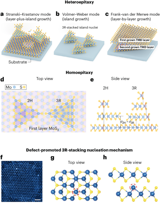
Liu, L. et al. Uniform nucleation and epitaxy of bilayer molybdenum disulfide on sapphire. Nature 605, 69–75 (2022).
Google Scholar
Wang, Q. et al. Layer-by-layer epitaxy of multi-layer MoS2 wafers. Natl Sci. Rev. 9, nwac077 (2022).
Google Scholar
Yang, T. et al. Ferroelectric transistors based on shear-transformation-mediated rhombohedral-stacked molybdenum disulfide. Nat. Electron. 7, 29–38 (2024).
Google Scholar
Zhang, X. et al. Transition metal dichalcogenides bilayer single crystals by reverse-flow chemical vapor epitaxy. Nat. Commun. 10, 598 (2019).
Google Scholar
Deng, Y. et al. Controlled growth of 3R phase tantalum diselenide and its enhanced superconductivity. J. Am. Chem. Soc. 142, 2948–2955 (2020).
Google Scholar
Pan, Y. et al. Heteroepitaxy of semiconducting 2H-MoTe2 thin films on arbitrary surfaces for large-scale heterogeneous integration. Nat. Synth. 1, 701–708 (2022).
Google Scholar
Chang, C. et al. Remote epitaxy of single-crystal rhombohedral WS2 bilayers. Nat. Commun. 15, 4130 (2024).
Google Scholar
Qin, B. et al. Interfacial epitaxy of multilayer rhombohedral transition-metal dichalcogenide single crystals. Science 385, 99–104 (2024).
Google Scholar
Li, T. et al. Epitaxial growth of wafer-scale molybdenum disulfide semiconductor single crystals on sapphire. Nat. Nanotechnol. 16, 1201–1207 (2021).
Google Scholar
Puretzky, A. A. et al. Low-frequency Raman fingerprints of two-dimensional metal dichalcogenide layer stacking configurations. ACS Nano 9, 6333–6342 (2015).
Google Scholar
Liang, L. et al. Low-frequency shear and layer-breathing modes in Raman scattering of two-dimensional materials. ACS Nano 11, 11777–11802 (2017).
Google Scholar
Seol, M. et al. High-throughput growth of wafer-scale monolayer transition metal dichalcogenide via vertical Ostwald ripening. Adv. Mater. 32, 2003542 (2020).
Google Scholar
Strachan, J., Masters, A. F. & Maschmeyer, T. 3R-MoS2 in review: history, status, and outlook. ACS Appl. Energy Mater. 4, 7405–7418 (2021).
Google Scholar
Wang, L. et al. Epitaxial growth of a 100-square-centimetre single-crystal hexagonal boron nitride monolayer on copper. Nature 570, 91–95 (2019).
Google Scholar
Chen, T. et al. Wafer-scale single-crystal hexagonal boron nitride monolayers on Cu (111). Nature 579, 219–223 (2020).
Google Scholar
Yang, P. et al. Epitaxial growth of centimeter-scale single-crystal MoS2 monolayer on Au(111). ACS Nano 14, 5036–5045 (2020).
Google Scholar
Kang, K. et al. High-mobility three-atom-thick semiconducting films with wafer-scale homogeneity. Nature 520, 656–660 (2015).
Google Scholar
Zhang, X. et al. Defect-controlled nucleation and orientation of WSe2 on hBN: a route to single-crystal epitaxial monolayers. ACS Nano 13, 3341–3352 (2019).
Google Scholar
Zhang, F. et al. Full orientation control of epitaxial MoS2 on hBN assisted by substrate defects. Phys. Rev. B 99, 155430 (2019).
Google Scholar
Li, J. et al. General synthesis of two-dimensional van der Waals heterostructure arrays. Nature 579, 368–374 (2020).
Google Scholar
Addou, R. et al. Impurities and electronic property variations of natural MoS2 crystal surfaces. ACS Nano 9, 9124–9133 (2015).
Google Scholar
Ferreira, F. et al. Adsorption of H2, O2, H2O, OH and H on monolayer MoS2. J. Phys. Condens. Matter 30, 035003 (2018).
Google Scholar
Hong, J. et al. Exploring atomic defects in molybdenum disulphide monolayers. Nat. Commun. 6, 6293 (2015).
Google Scholar
Konabe, S. & Yamamoto, T. Piezoelectric coefficients of bulk 3R transition metal dichalcogenides. Jpn. J. Appl. Phys. 56, 098002 (2017).
Google Scholar
Wang, J. et al. Logic and in-memory computing achieved in a single ferroelectric semiconductor transistor. Sci. Bull. 66, 2288–2296 (2021).
Google Scholar
Wang, L. et al. Exploring ferroelectric switching in α–In2Se3 for neuromorphic computing. Adv. Funct. Mater. 30, 2004609 (2020).
Google Scholar
Baek, S. et al. Ferroelectric field-effect-transistor integrated with ferroelectrics heterostructure. Adv. Sci. 9, e2200566 (2022).
Google Scholar
Wang, S. et al. Two-dimensional ferroelectric channel transistors integrating ultra-fast memory and neural computing. Nat. Commun. 12, 53 (2021).
Google Scholar
Xue, F. et al. Giant ferroelectric resistance switching controlled by a modulatory terminal for low-power neuromorphic in-memory computing. Adv. Mater. 33, e2008709 (2021).
Google Scholar
Singh, P. et al. Two-dimensional CIPS-InSe van der Waal heterostructure ferroelectric field effect transistor for nonvolatile memory applications. ACS Nano 16, 5418–5426 (2022).
Google Scholar
Liao, J. et al. Van der Waals ferroelectric semiconductor field effect transistor for in-memory computing. ACS Nano 17, 6095–6102 (2023).
Google Scholar
Bao, Y. et al. Gate-tunable in-plane ferroelectricity in few-layer SnS. Nano Lett. 19, 5109–5117 (2019).
Google Scholar
Kwon, K. C. et al. In-plane ferroelectric tin monosulfide and its application in a ferroelectric analog synaptic device. ACS Nano 14, 7628–7638 (2020).
Google Scholar
Blöchl, P. E. Projector augmented-wave method. Phys. Rev. B 50, 17953–17979 (1994).
Google Scholar
Kresse, G. & Furthmüller, J. Efficient iterative schemes for ab initio total-energy calculations using a plane-wave basis set. Phys. Rev. B 54, 11169–11186 (1996).
Google Scholar
Perdew, J. P., Burke, K. & Ernzerhof, M. Generalized gradient approximation made simple. Phy. Rev. Lett. 77, 3865–3868 (1996).
Google Scholar
Grimme, S., Antony, J., Ehrlich, S. & Krieg, H. A consistent and accurate ab initio parametrization of density functional dispersion correction (DFT-D) for the 94 elements H-Pu. J. Chem. Phys. 132, 154104 (2010).
Google Scholar
Ming, W., Huang, B. & Li, J. Decoupling competing electromechanical mechanisms in dynamic atomic force microscopy. J. Mech. Phys. Solids 159, 104758 (2022).
Google Scholar
Chen, Q. N., Ou, Y., Ma, F. & Li, J. Mechanisms of electromechanical coupling in strain based scanning probe microscopy. Appl. Phys. Lett. 104, 242907 (2014).
Google Scholar
Jungk, T., Hoffmann, Á. & Soergel, E. Quantitative analysis of ferroelectric domain imaging with piezoresponse force microscopy. Appl. Phys. Lett. 89, 163507 (2006).
Google Scholar
Lobato, I. & Van Dyck, D. MULTEM: a new multislice program to perform accurate and fast electron diffraction and imaging simulations using graphics processing units with CUDA. Ultramicroscopy 156, 9–17 (2015).
Google Scholar
Li, W. et al. Approaching the quantum limit in two-dimensional semiconductor contacts. Nature 613, 274–279 (2023).
Google Scholar
Jerry, M. et al. Ferroelectric FET analog synapse for acceleration of deep neural network training. In IEEE International Electron Devices Meeting (IEDM) 6.2.1–6.2.4 (IEEE, 2017).
Beeche, C. et al. Super U-Net: a modularized generalizable architecture. Pattern Recognit. 128, 108669 (2022).
Google Scholar
Zhao, P. et al. A new method for classifying and segmenting material microstructure based on machine learning. Mater. Des. 227, 111775 (2023).
Google Scholar
Bangaru, S. S., Wang, C., Zhou, X. & Hassan, M. Scanning electron microscopy (SEM) image segmentation for microstructure analysis of concrete using U-net convolutional neural network. Autom. Constr. 14, 104602 (2022).
Google Scholar